Transparent conducting films (TCFs) are widely used in modern electronic devices. These thin, conductive films can carry electricity when deposited on glass, silicon or polymer substrate. TCFs are used as electrodes for OLED and solar cells or simply as the conductive layers on the touch screen of your favorite phone.

In the TCF family, indium tin oxide (ITO) is the industry standard due to its excellent transparency and electrical properties. Recent materials like graphene oxide (GO) or PEDOT show great promise for flexible electronics since they are more prone to bending than ITO.
Patterning of transparent conductive films
The patterning of these conductive layers is a very important manufacturing process that allows to remove some parts of the layer to functionalize the surface electrical properties and create electrical circuits on the layer depending on the application. Laser patterning is a promising approach as compared to photolithography as it gives the flexibility to customize the patterning with very high throughputs while eliminating the use of consumables and pre-processing steps.
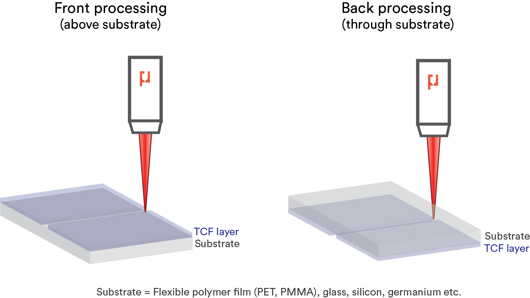
One of the biggest challenges when it comes to laser patterning of TCFs is the ability to selectively remove the thin film without affecting the underlying substrate (glass, polymer, silicon, etc.). Depending on the deposition process or the application, it may be also preferable to remove the TCF layer above the substrate (front processing) or through the substrate (back processing), as shown in Figure 2.
Mid-infrared selective laser patterning of thin films
To overcome these challenges, Femtum developed a new mid-IR pulsed fiber laser at 2.8 µm for selective removal of transparent conductive films on different substrates.
Mid-IR pulsed lasers are ideal for thin film patterning because most conductive thin films are based on oxide materials that strongly absorb at wavelength around 3 µm. As compared to UV or near-IR laser patterning, it is easier to selectively remove these thin layers without affecting the substrate, which possess a much higher ablation threshold at these mid-IR wavelengths.
Figure 3 shows an example of ITO patterning on PET with the Femtum Nano 2800 using both front and back processing methods.
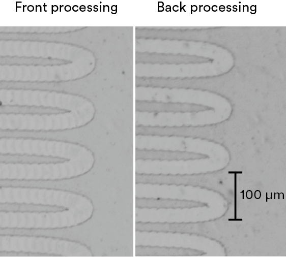
Due to the excellent beam quality of the Femtum Nano 2800, precise patterning with small feature size (around 10 µm) can also be achieved, as shown in Figure 4.

The ability to process TCFs on various substrates like flexible polymers (PET, PMMA, Polyimide, etc.) or other mid-IR transparent substrates (silicon, germanium) with this versatile, turn-key industrial fiber laser opens up a wide range of applications from flexible displays to wearable sensors.
If you are interested to learn more about the process or to test the laser for your manufacturing process, please Contact us.