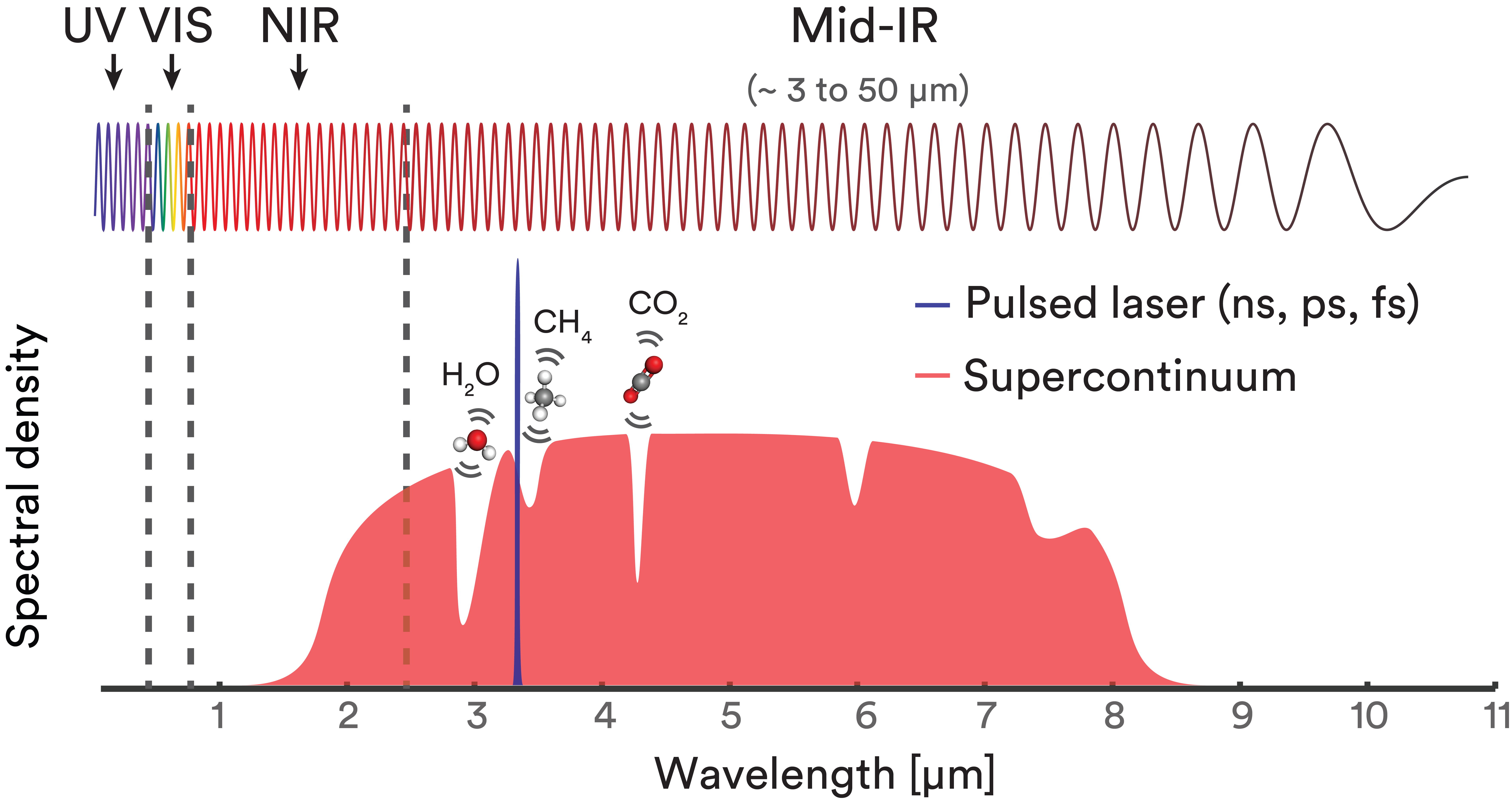
Choosing the right optical elements for your mid-infrared laser applications
Laser systems operating in near infrared (from 0.75 μm to 1 μm) and short-wave infrared (between 0.9 μm and 2.5 μm) are widely used in many applications. As a result, laser experts are well acquainted with the common optical components such as lenses, windows, beam splitters, mirrors, polarizers and filters. Materials such as fused silica, BK7,…